Build this Joystick! Electrical build up.
Now available:
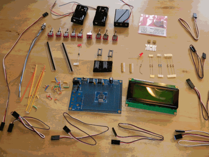
Electrical components. Here is the components for the full version. As can be seen there is the parallax display and the amount of switches that are the main differences from the simpler version.
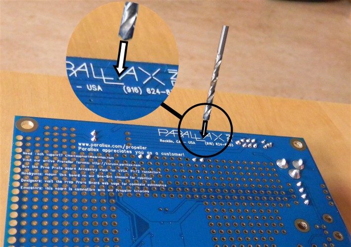
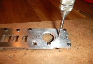
Drill point on card. Drill away some material to disconnect the leader between the upper and the lower side of the card. A suitable drill would be somewhat about 2,5mm. N.B.! The point is to be located at the end of one track at the underside (a seen by picture). Do not locate it by means of the printed text on board, the position of the text can differ between boards!
Click on picture for bigger version!
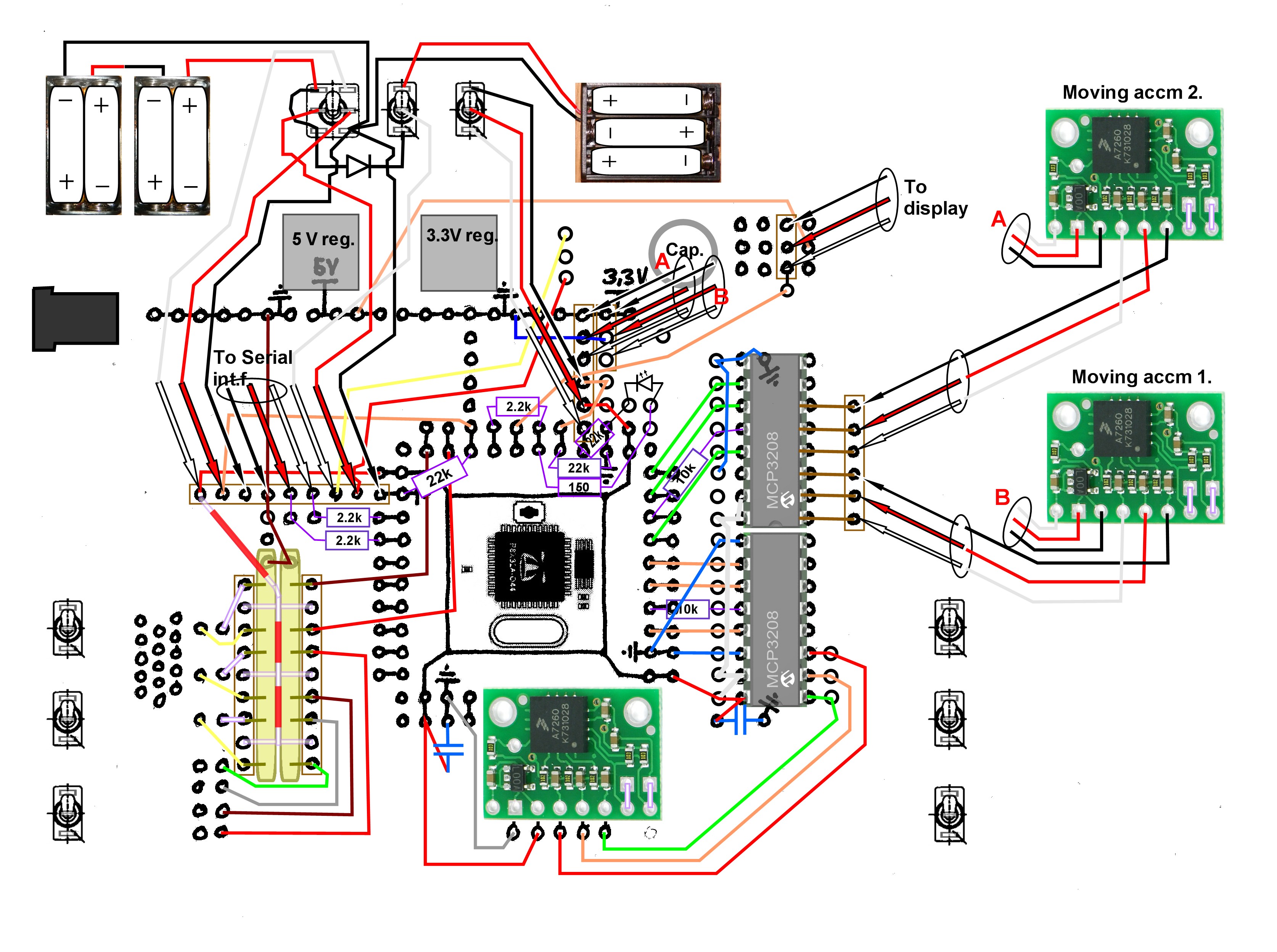
Scheme. This scheme is presented somewhat special. It shows the wires as placed on the parallax proto board. Therefor not all connections to the processor are shown. They are simply pre print on board. (Do also see parallax documentation of board). N.B. that not all individual parts are drawn to the same scale. For example the battery holders are drawn at a smaller scale. The color of the wires are the same as in the pictures in this description. Where wires also act as jumpers on bottom side of board this is indicated with the same color although this part of wire is naked in reality! White wires are shown in a pale gray color. Orange wire connecting 5V to display connector (top right) is to be placed on bottom side.
Only used holes are shown to make the view more clear.
Brown rectangles denote connectors placed at the bottom side of the board.
Long rectangular brown and yellow items are thick film resistors. Nine resistors in one package with ten legs (common earth). Out of these ten legs three are to be cut away. Together with the thick film resistors is drawn a small grid of jumpers (violet and red color). These are to be placed on bottom side.
Both capacitors denoted by blue symbols are 0.1uF. Note that the power supply (A and B with red letters) for the moving accelerometers have the color of the leaders inverted from convenient ( +3.3V has black wire and earth has red wire). The reason for this is that the three part ribbon cableconnector from parallax have that order of colors.
Six of the switches do not have their connections shown. They are shown in the next detail:
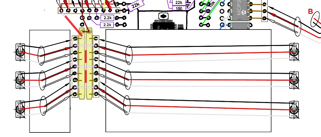
In this picture parts of the main scheme has been masked away: (white rectangles). Now the ribbon cables can be shown. To observe: Wires are shown from above but go to the connectors at bottom side of board. One three part cable to each switch. Now this is a suggestion, you may self decide to place switches in another order or with mirrored function. And of course you may always change in the program to redefine what pin will belong to what switch (function).
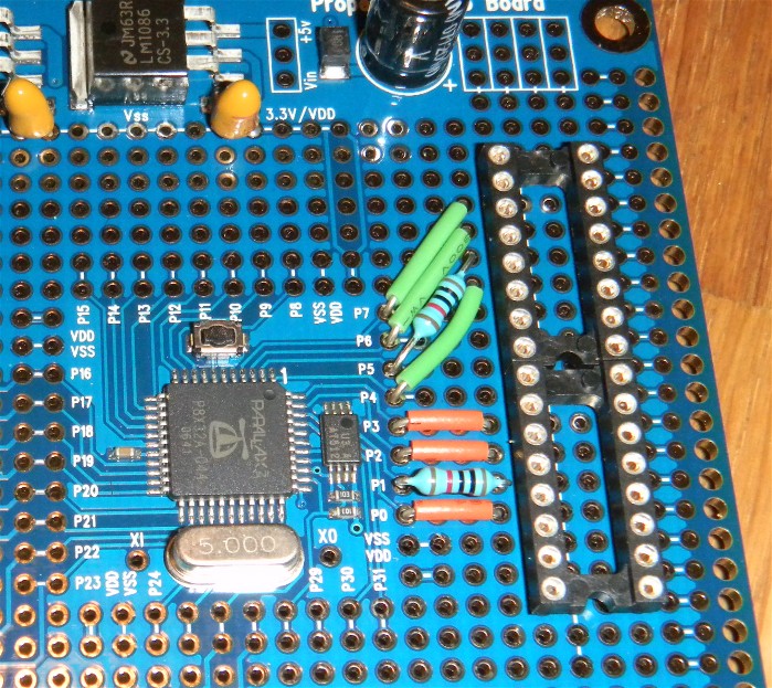
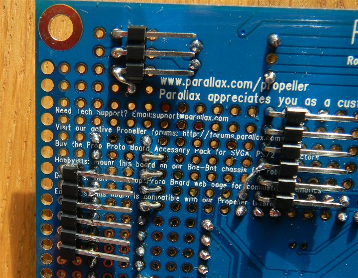
Start placing out components. I suggest to start with the IC-holders for the AD:s. As seen in picture place one of the holders with its "no 1" pin in the same row as P31 indicated on board. Let there be two columns left next to right of the holder. The holder should ride over the Vss column marked by a white line. Place the next holder direct adjacent to the first one. Then place the first resistors and jumpers as indicated in picture. Note that each leg protruding the board close to the holder should be long enough to be bent and connected to the closest pin on the IC-holder. Solder all Items.
Next step is to adjust the thick film resistors a little. They consist of nine resistors each but we will only use six. So 3 legs has to be cut away not to connect earth to the wrong point. We are only interested in the form the resistors comes in, not in all resistors.
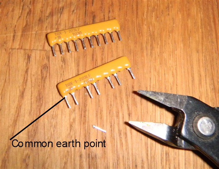
Cut away three legs on each resistor as seen. Unaffected resistor in top. Note that the common earth point is situated at the end where the text is most close. Not to cut the wrong legs away. Install the resistors as seen in next picture. Common earth point pointing to the top of picture.
Here more components have been mounted. The long yellow items are thick film resistors. Their legs protrude the board and are bent to connect to the two rows of angled connector pins soldered to the bottom side of the board. Note that 3 legs on each resistor have been cut away! Do also note jumpers placed to the left. Both naked wire (3 pieces) and 3 yellow ones. Don’t mind about the printed text saying "Mouse" on board. In this application this function is not used – used are only the pre print leaders connecting this area with the processor. The two resistors connected to P16 and P17 are for the in/out interface and 2.2k Ohm each.
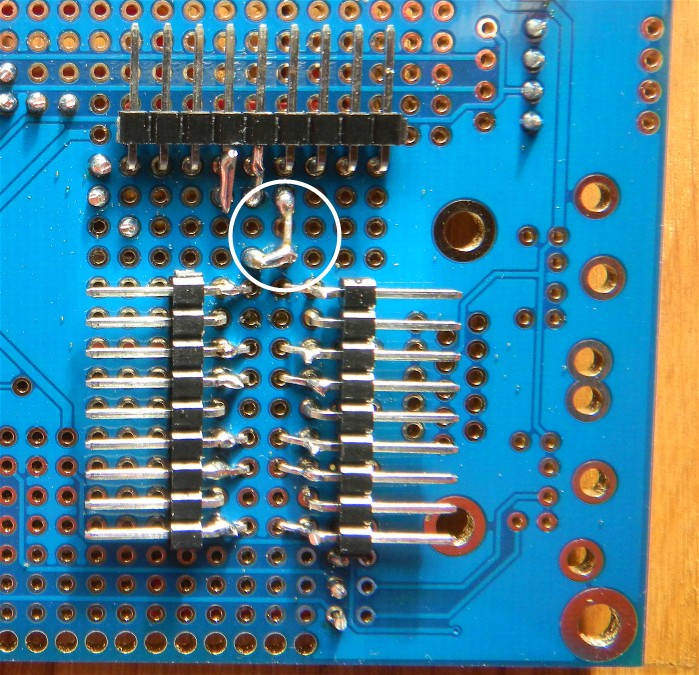
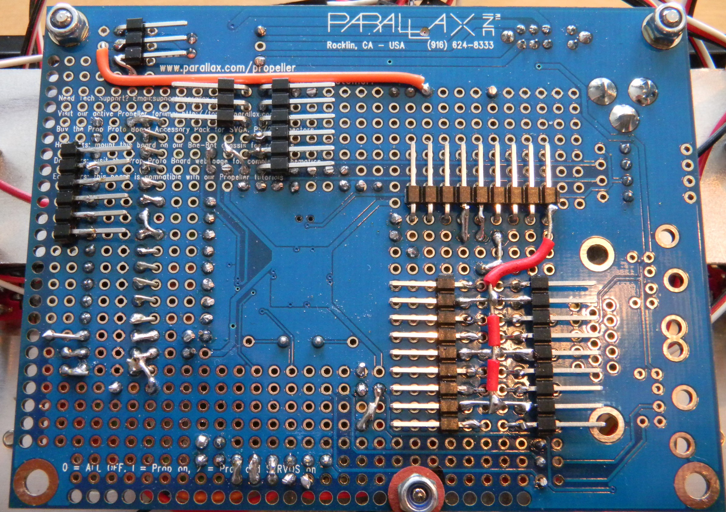
Above described area from under side. Two rows of angled connectors 3X2.54 mm (3X0.1"") apart from each other. One more row at top of picture. Between the two lower rows there can be seen 2X6 legs that origin from the thick film resistors at the top side. The last two legs of the resistors are connected to each other and then joined to earth (Vss) by a jumper (circled area).
Do also see the top view (former picture) where the jumper goes on in a brown coating.
Now this area is not fully complete. There will also be wiring for 3.3V (Vdd) added. Shown in a picture further down.
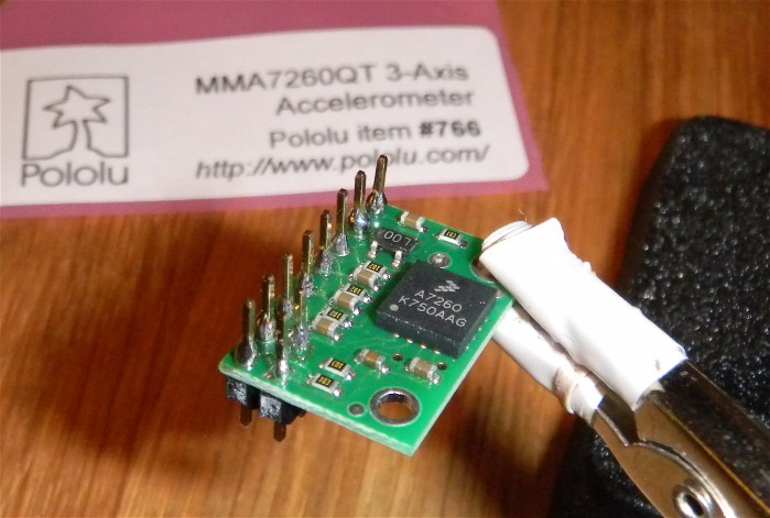
Solder the pins to the first accelerometer break out board. The pins should protrude from underside so that the plastic distance is situated at the underside. This only applies to the accelerometer to be placed on the proto board.
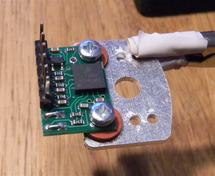
Then solder the pins to the two accelerometers to be placed with the moving axles. The pins should be soldered with the plastic distances on the upper side. Only six pins are mounted. At the last places jumpers are placed as shown in picture. Do also mount the accelerometer on the small aluminum console made for the purpose. 2,5mm screws with metric thread should be used. The threads in the console will be easily made by just screwing the screw into the precut hole. The hole in the accelerometer break out board can be a little tight but just screw the screw in and it will work. N.B. First screw into aluminum to provide thread, then mount board.
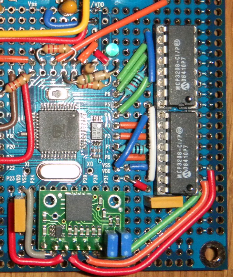
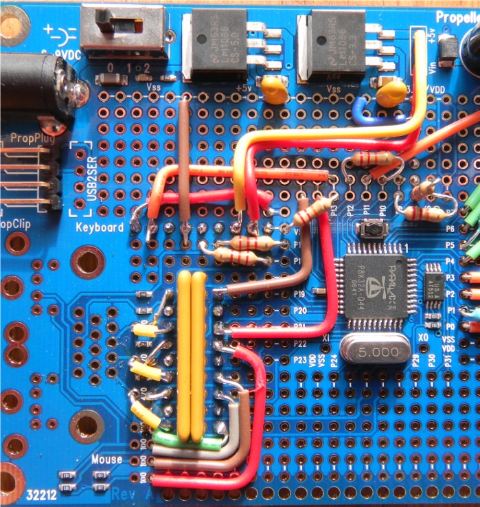
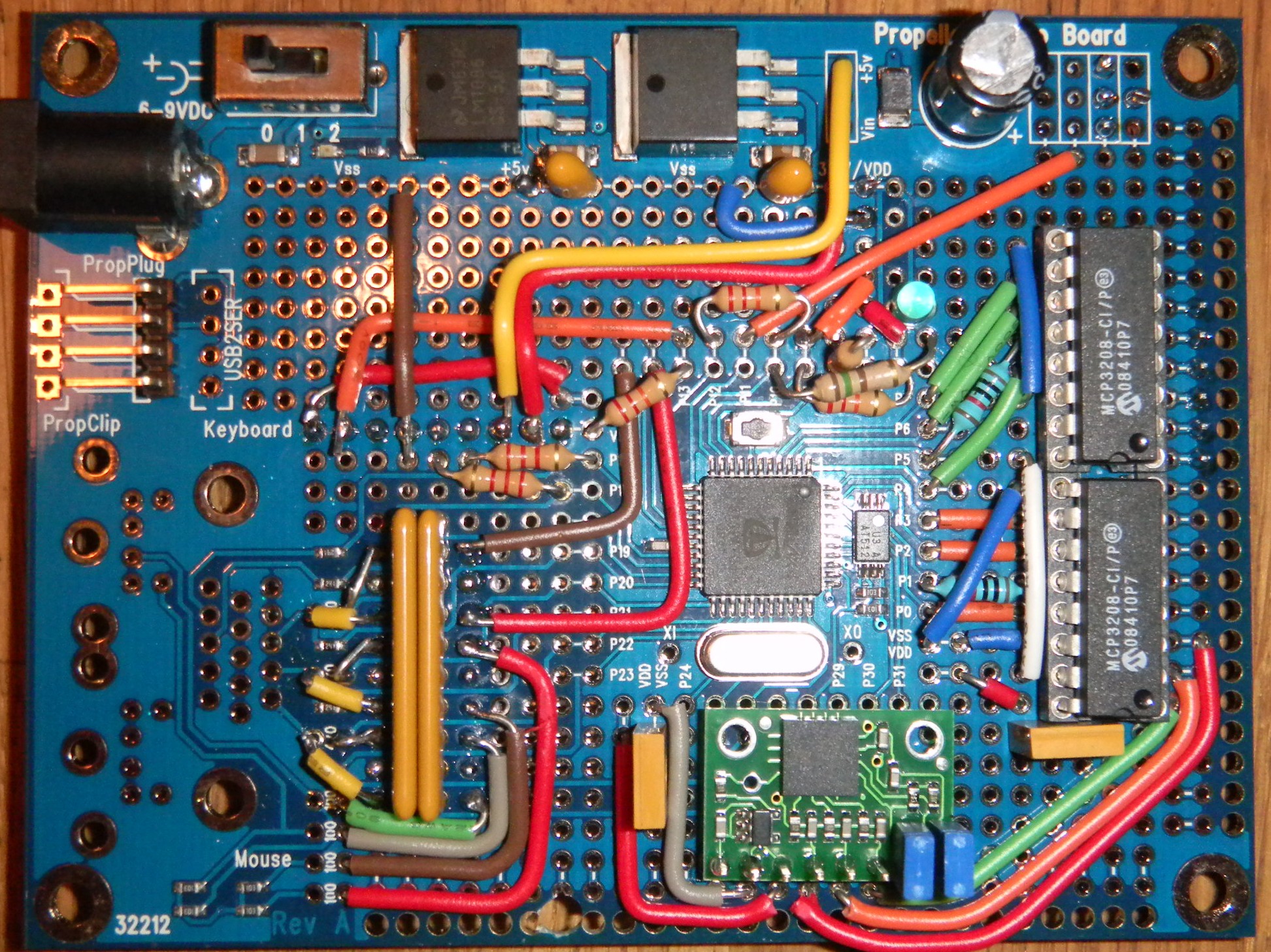
Mount the board fixed accelerometer to the board. Placement as seen in picture. The small board is only fixed by means of the soldered connecting pins. No screws are used. Try to mount as parallel to main board as possible. To the left are power supply; Grey is Vss and red Vdd (3.3V). The orange-yellow item is a 0,1m F capacitor. The three next wires are x, y and z analog outputs from the accelerometer. The two blue items are detachable jumpers. At the AD area the circuit have been completed with leaders for power supply and reference voltage (same as power supply). There has also been mounted a capacitor. Near top of the picture have been added a LED (blue) and a resistance (150 ohms) for the LED. There have also been added some wires for the mode select function (short red and orange jumpers). In the picture the AD:s are seen mounted in their holders. Do wait with this until the board is complete. They are probably the most sensitive component so you better wait with mounting as long as possible. Do also see scheme.
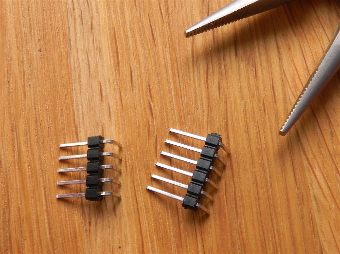
Use a pair of pliers to relocate the plastic at a row of six angled connectors as seen. The left ones are original, the right ones are altered.
Solder the six connectors with relocated plastic distances so that they contact six of the IC holder pins as seen down to the left in picture. The short angled parts to go down into the holes.
Click on picture for bigger version.
Here can be seen the complete proto board from beneath. Note the orange wire in the upper part of the picture. This is to feed the LCD with 5 volts. Because of the split of the board at the drill point described earlier the feed connection is also split. Therefor the wire is needed.
N.B. the red jumper feeding right-lower connector area with 3.3V. Do also note the small jumpers (naked wire) soldered to the red one.
Click on card for higher res.
Complete card upper side. Note blue jumpers on card mounted accelerometer break out board. They are delivered with the board but can be replaced with soldered jumpers.
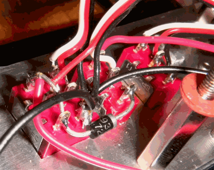
This is a blow up of the on/off switch area. On off switch in the middle. Display switch to the left and mode switch to the right. Note diode running from one switch to another and also connecting two electrodes on the left switch. Immediately behind the diode body the common earth electrode is situated gathering four wires at one point. Also look at scheme.
Mechanical description Function and code